Hongke Case
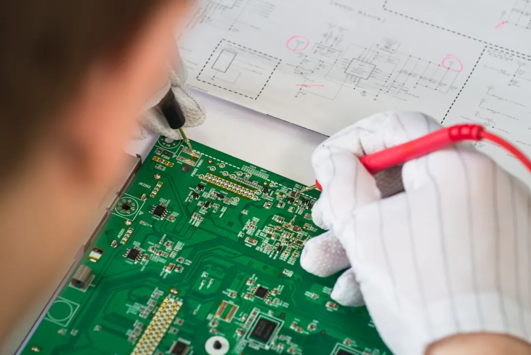
【虹科方案】AI+AR 重塑 PCB 質控流程|虹科 AR 智慧質檢解決方案
虹科結合 AR 智慧眼鏡與 AI 辨識技術,打造標準化 PCB 質檢工作流程,整合 MES、ERP、AOI 系統,降低漏檢率、提升良率,加速電子製造數位化升級。

Lorem ipsum dolor sit amet, consectetur adipiscing elit. Ut elit tellus, luctus nec ullamcorper mattis, pulvinar dapibus leo.
Lorem ipsum dolor sit amet, consectetur adipiscing elit. Ut elit tellus, luctus nec ullamcorper mattis, pulvinar dapibus leo.
As Micro-LED display technology and advanced semiconductor components continue to push the limits of miniaturization and high performance, the process of Accuracy and Scalability It's more critical than ever. Technology leader Micraft Systems Plus has developed two future-proof high-end machines:
Micro-LED Laser Welder and HBM High Precision Wafer LaminatorThe
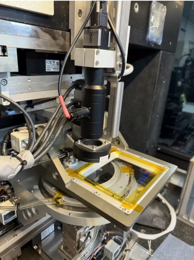
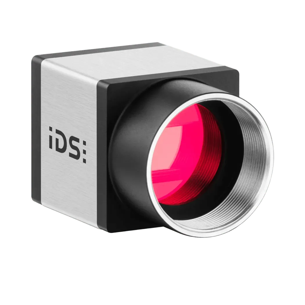
Both systems utilize USB3 uEye CP Series Industrial Camera from IDS, a co-brand of HTCThe system is designed to achieve the ultimate in precision, speed and process control. It has already been deployed in volume in the Asian electronics manufacturing market.
The Micro-LED laser soldering machine is designed for high speed and accurate transfer operations on large substrates (e.g. G4.5, G6 glass). Laser welding minimizes thermal and mechanical stresses, and is especially suited for applications where thousands of micro components are handled simultaneously.
The camera is first responsible for acquiring global datum marks to establish the relative position of the substrate in the machine's coordinate system; the positioning information is then transmitted to the motion control system so that the overall mechanism can be ±1 µm repeatability Completes high-precision movements.
After the fitting stage, the camera performs datum acquisition to realize the Real-time sub-micron alignmentIt also automatically performs dynamic rotation correction when necessary. This critical information guides the motion system to make position/angle corrections to ensure that each Micro-LED is perfectly aligned with the target pixel.
This system has a capacity of up to 10 million wafers per hour (cph).The combination of extremely high precision and large-scale mass production capability is an important KPI for expanding Micro-LED volume production.
The camera can automatically move to the inspection area to assist the operator with quick quality confirmation, including:
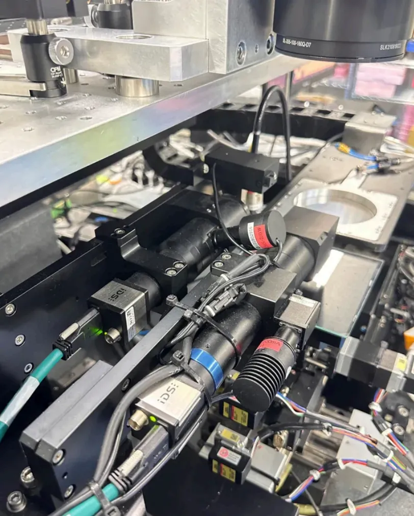
The IDS USB3 uEye CP camera (model U3-3800CP-M-GL Rev. 2.2), a co-brand of Avision, plays a key role in supporting the entire Micro-LED production process:
Damien Wang, IDS Regional Manager for Asia Pacific, said:"High-resolution and low-noise images capture even the smallest imperfections and are essential for high-precision processes."
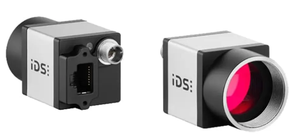
The U3-3800CP utilizes the Sony STARVIS IMX183 (20.44 megapixels, 2.4 µm pixel size, 19.8 fps) to maintain excellent image quality in low light and high-speed scenes.
HBM's advanced wafer laminators are designed for high-density semiconductor packaging, especially for vertical stacking (3D stacking) processes that require micron-level precision.
The system is operated with two IDS U3-3890CP-M-GL Rev.2.2:
After the camera captures the data, the motion control system completes the precision alignment, ensuring consistent solder joints and avoiding thermal or electrical problems caused by micron-level deviations, even in high-density packages such as HBM.
The U3-3890CP features the Sony STARVIS IMX226 (12 megapixels, 1.85 µm pixel size, 33.2 fps), featuring:
Ideal for high-precision visual positioning required in 2.5D and 3D packaging.
Both devices utilize the uEye CP series and features include:
By integrating IDS vision technology, manufacturers gained:
These two systems have been deployed in many top manufacturing enterprises in Taiwan and Asia, demonstrating the best combination of German high-end vision technology and advanced automation systems.
虹科結合 AR 智慧眼鏡與 AI 辨識技術,打造標準化 PCB 質檢工作流程,整合 MES、ERP、AOI 系統,降低漏檢率、提升良率,加速電子製造數位化升級。
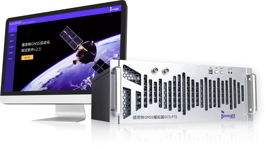
深入解析虹科 GNSS 模擬器如何支援無人機整機測試,涵蓋多星座 GNSS 仿真、RTK 公分級定位、抗干擾測試與多感測器融合驗證,助力高效、安全的 UAV 研發。
增材製造(PBF-LB/M)中的高精度過程監控與誤差檢測,虹科 iDS USB3 工業相機助力粉末層、再熔化層與動態飛濺監控,提升部件品質與研發效率,適用航空航天、醫療、汽車等行業。