
Search

Hongke's latest articles

HongKe

Lorem ipsum dolor sit amet, consectetur adipiscing elit. Ut elit tellus, luctus nec ullamcorper mattis, pulvinar dapibus leo.

Lorem ipsum dolor sit amet, consectetur adipiscing elit. Ut elit tellus, luctus nec ullamcorper mattis, pulvinar dapibus leo.

IDS Precision Vision System for Micro-LED Lamination and HBM Packaging Process Upgrades

As Micro-LED display technology and advanced semiconductor components continue to push the limits of miniaturization and high performance, the process of Accuracy and Scalability It's more critical than ever. Technology leader Micraft Systems Plus has developed two future-proof high-end machines:
Micro-LED Laser Welder and HBM High Precision Wafer LaminatorThe

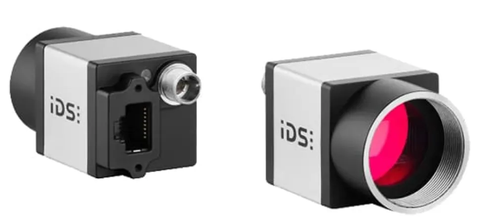
Both systems utilize USB3 uEye CP Series Industrial Camera from IDS, a co-brand of HTCThe system is designed to achieve the ultimate in precision, speed and process control. It has already been deployed in volume in the Asian electronics manufacturing market.

1. Application Scenario 1: 20 Megapixel USB3 uEye CP Camera Supports Micro-LED Transfer and Laser Soldering Processes

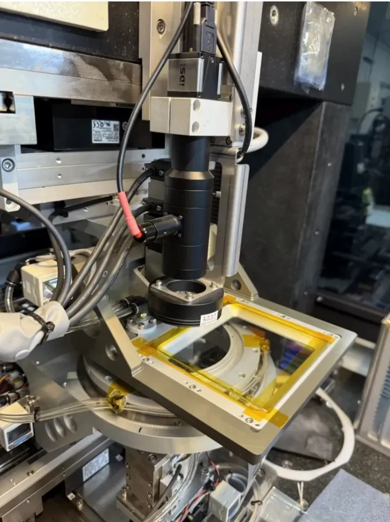
The Micro-LED laser soldering machine is designed for high speed and accurate transfer operations on large substrates (e.g. G4.5, G6 glass). Laser welding minimizes thermal and mechanical stresses, and is especially suited for applications where thousands of micro components are handled simultaneously.

Substrate positioning and precision motion control

The camera is first responsible for acquiring global datum marks to establish the relative position of the substrate in the machine's coordinate system; the positioning information is then transmitted to the motion control system so that the overall mechanism can be ±1 µm repeatability Completes high-precision movements.

Fine-tuning and Dynamic Alignment

After the fitting stage, the camera performs datum acquisition to realize the Real-time sub-micron alignmentIt also automatically performs dynamic rotation correction when necessary. This critical information guides the motion system to make position/angle corrections to ensure that each Micro-LED is perfectly aligned with the target pixel.

This system has a capacity of up to 10 million wafers per hour (cph).The combination of extremely high precision and large-scale mass production capability is an important KPI for expanding Micro-LED volume production.

Built-in In-line Inspection

The camera can automatically move to the inspection area to assist the operator with quick quality confirmation, including:

  • Accurate wafer lamination
  • Is there any tilting, breakage
  • Are there any mismatches or anomalies

Industrial cameras are the "visual core" of the process

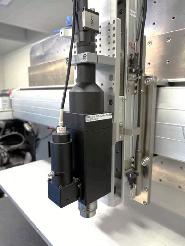
The IDS USB3 uEye CP camera (model U3-3800CP-M-GL Rev. 2.2), a co-brand of Avision, plays a key role in supporting the entire Micro-LED production process:

  • Donor Wafer Inspection: Detecting defects such as breakage, missing parts, etc.
  • Mega Transfer AlignmentGrabbing substrate and wafer alignment marks for sub-micron placement
  • Post-transfer detection: Confirmation of positioning accuracy, tilt and breakage
  • Precision Rework (Rework): Assisting in micron single chip replacement

Damien Wang, IDS Regional Manager for Asia Pacific, said:"High-resolution and low-noise images capture even the smallest imperfections and are essential for high-precision processes."

The U3-3800CP utilizes the Sony STARVIS IMX183 (20.44 megapixels, 2.4 µm pixel size, 19.8 fps) to maintain excellent image quality in low light and high-speed scenes.

Application Scenario 2: 12 Megapixel USB3 uEye CP supporting HBM (High Bandwidth Memory) Chip Bonding

HBM's advanced wafer laminators are designed for high-density semiconductor packaging, especially for vertical stacking (3D stacking) processes that require micron-level precision.

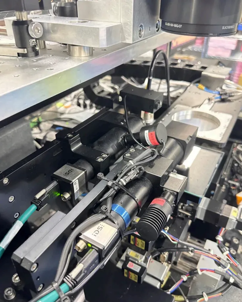
The system is operated with two IDS U3-3890CP-M-GL Rev.2.2:

  • Alignment of wafers and pads
  • Alignment Coordinate Conversion
  • Guided Lamination Modules for Micron-Scale Placement

Sub-micron bonding accuracy

After the camera captures the data, the motion control system completes the precision alignment, ensuring consistent solder joints and avoiding thermal or electrical problems caused by micron-level deviations, even in high-density packages such as HBM.

CMOS Sensor for Wafer Lamination

The U3-3890CP features the Sony STARVIS IMX226 (12 megapixels, 1.85 µm pixel size, 33.2 fps), featuring:

  • high sensitivity
  • low-noise signaling
  • High Speed Response

Ideal for high-precision visual positioning required in 2.5D and 3D packaging.

IDS uEye CP Series: The Common Vision Core for Both Systems

Both devices utilize the uEye CP series and features include:

  • Ultra compact 29 × 29 × 29 mm Magnesium alloy housing
  • USB3 Vision High Speed Transmission
  • Global Shutter CMOS
  • Supports BSI back-illuminated STARVIS technology in low light environments.
  • High resolution, low noise, ideal for recognizing micron markers/solder balls
  • High thermal stability for 24/7 continuous operation in semiconductor fabs
  • Built-in 120 MB of buffer memory to optimize multi-phase usage
  • Supports IDS full software SDK to accelerate system integration

Customer Benefits: Scalable High Precision and Higher Capacity

By integrating IDS vision technology, manufacturers gained:

  • Higher fit and alignment accuracy
  • Better process repeatability
  • More stable long-term production performance
  • Lower error rate and shorter setup time
  • Significantly increased capacity and process yields

These two systems have been deployed in many top manufacturing enterprises in Taiwan and Asia, demonstrating the best combination of German high-end vision technology and advanced automation systems.

Other Articles

Hongke Case

[Hongke Solutions] Safety Solution for Long-Distance Ocean Transport of Lithium Batteries – Shengweino International Case Study

How Can Thermal Runaway and Impact Damage Be Prevented During Long-Distance Ocean Transport of Lithium-Ion Batteries? Shengweino International uses Hongke’s ASPION G-Log 2 shock recorder to precisely monitor container impacts (G-forces) and changes in temperature and humidity throughout the entire journey, creating a comprehensive transport environment history and improving the efficiency of logistics claims processing and quality tracking. Learn more about our B2B lithium-ion battery ocean freight safety monitoring solutions now!

Read more
Hongke Dry Goods

[Hongke Solutions] Cybersecurity Training for Hong Kong’s Financial Industry: From Compliance Records to Human-Factor Risk Management

Cybersecurity Training Solutions for Hong Kong Financial Institutions (Banks, Securities Firms, and Insurance Companies). Designed to meet the compliance requirements of the Hong Kong Monetary Authority (HKMA) and the Securities and Futures Commission (SFC), these solutions help prevent Business Email Compromise (BEC), OTP phishing, and deepfake attacks. Utilizing KnowBe4’s automated simulation exercises, this solution establishes a human-factor risk management mechanism with a complete audit trail.

Read more
Hongke Case

[Hongke Applications] Hongke IDS Multi-Camera Imaging Solution – Overcoming the Challenge of Precise 3D Observation of High-Speed Dynamic Plasma

Hongke, in collaboration with IDS, offers a multi-camera synchronized imaging solution featuring microsecond-level ultra-short exposure and back-illuminated global shutter CMOS sensors, successfully overcoming bottlenecks in high-speed, microscale plasma 3D point cloud reconstruction and dynamic observation. Learn more about Hongke’s industrial machine vision solutions today!

Read more

Contact Hongke to help you solve your problems.

Let's have a chat